CuriousTab |
CuriousTab
Discussion
Home ‣ Digital Electronics ‣ Combinational Logic Circuits Comments
- Question
Options- Correct Answer
- An open input on the first IC chip on the board
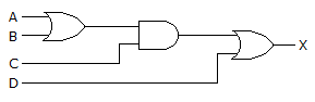
- 1. Solve the network in the figure given below for X.
Options
Discuss
- 3. For the device shown here, assume the D input is LOW, both S inputs are HIGH, and the
 input is HIGH. What is the status of the
  outputs?
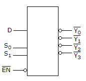
Options- C. All but
 are LOW.
 - D. All but
 are HIGH.
Discuss
are HIGH.
Discuss
- 7. For the device shown here, assume the D input is LOW, both S inputs are LOW, and the input is LOW. What is the status of the outputs?

Options- C. All but
 are LOW.
 - D. All but
 are HIGH.
Discuss
are HIGH.
Discuss
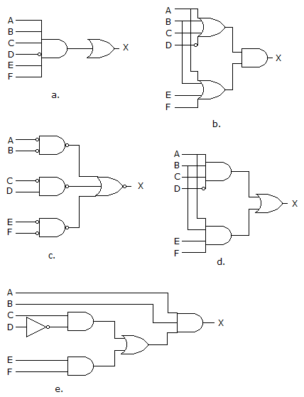
- 9. Which of the circuits in figure (a to d) is the sum-of-products implementation of figure (e)?
Options
Discuss
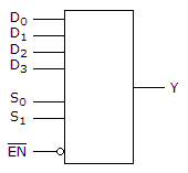
- 10. For the device shown here, let all D inputs be LOW, both S inputs be HIGH, and the input be LOW. What is the status of the Y output?
Options
Discuss
Combinational Logic Circuits problems
Search Results
Correct Answer: ((A + B)C) + D
Correct Answer: All are HIGH.
Correct Answer: All but
are HIGH. Correct Answer: d
Correct Answer: LOW
Comments
There are no comments.