logo

CuriousTab

CuriousTab

Discussion


Home Digital Electronics MSI Logic Circuits Comments

  • Question
  • Which statement best describes the given figure, and what is the function of the terminal labeled EN?
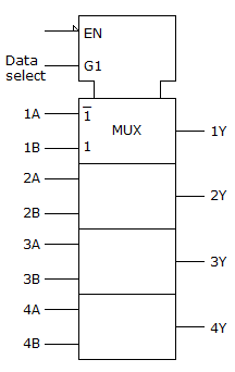
    Which statement best describes the given figure, and what is the function of the terminal labeled EN


  • Options
  • A. Quad two-input multiplexer. EN is the enable input, which requires an active LOW for the device to work.
  • B. Quad two-bit multiplier, EN is the active HIGH trigger.
  • C. Dual quad-input multiplexer, which requires an active LOW on the EN terminal for the device to work.
  • D. Quad two-input AND gate, which requires an active LOW on the EN input to enable all the gates.

  • Correct Answer
  • Quad two-input multiplexer. EN is the enable input, which requires an active LOW for the device to work. 


  • MSI Logic Circuits problems


    Search Results


    • 1. Refer to the figure given below. The logic function generator being implemented with the multiplexer in this circuit produces a constant LOW on the output. The ABC inputs are checked and appear to be pulsing; also, the 0?7 and EN inputs are checked with the scope and all appear to be at 0 V. A check with the DMM confirms that power is on. What is the problem, and what should be done to correct it?


    • Options
    • A. The output is shorted to Vcc; replace the IC.
    • B. The scope's vertical input is in the AC mode and the common connection for the 0,2,3 and 5 inputs is bad. Set the scope's vertical input mode to DC, and repair the bad solder connection.
    • C. Power has not been applied to the circuit; apply power.
    • D. The output is shorted to ground; replace the IC.
    • Discuss
    • 2. What are the outputs of a 7485 four-bit magnitude comparator when the inputs are A = 1001 and B = 1010?

    • Options
    • A. A < B is 1
      A = B is 0
      A > B is 1
    • B. A < B is 0
      A = B is 1
      A > B is 0
    • C. A < B is 0
      A = B is 0
      A > B is 1
    • D. A < B is 1
      A = B is 0
      A > B is 0
    • Discuss
    • 3. The data transmission system shown in below has a problem; the parity error output is always high. A logic analyzer is used to examine the system and shows that the DATA IN on the left matches the DATA OUT on right. What might be causing the problem?


    • Options
    • A. The error gate could be defective.
    • B. The storage circuit could be defective.
    • C. The parity checker could be bad.
    • D. Any of the above.
    • Discuss
    • 4. Why are control inputs included in an HDL magnitude comparator?

    • Options
    • A. For cascading the chips
    • B. For control signal input
    • C. For signal control
    • D. For internal interconnections
    • Discuss
    • 5. The BCD/DEC decoder shown in figure (a) is examined with a logic analyzer and the results are shown in the waveforms in figure (b). What, if anything, is wrong with the circuit?


    • Options
    • A. The "2" output is shorted to Vcc.
    • B. The A1 input is internally open.
    • C. The A1 input node is internally stuck LOW.
    • D. Nothing is wrong with the circuit.
    • Discuss
    • 6. What is the purpose of a decoder's inputs?

    • Options
    • A. To allow the decoder to respond to the inputs to activate the correct output gate.
    • B. To disable the decoder outputs so that all outputs will be inactive.
    • C. To disable the inputs and activate all outputs.
    • D. To allow the decoder to respond to the inputs to activate the correct output gate, and to disable the inputs and activate all outputs.
    • Discuss
    • 7. Referring to the figure given below, what output code will appear on the output (A3,A2,A1,A0) when the 5 key is pressed?


    • Options
    • A. 1010
    • B. 0101
    • C. 1101
    • D. 1011
    • Discuss
    • 8. It is suspected that the comparator in the figure given below has a problem. The inputs are activated in the table shown below and the corresponding outputs noted. What is most likely wrong with the circuit?
      For P0 ? P3 = 1 and Q0 ? Q3 = 0, P > Q = 1, P = Q = 1, P < Q = 0
      For P0 ? P3 = 0 and Q0 ? Q3 = 1, P > Q = 0, P = Q = 1, P < Q = 1
      For P0 ? P3 = 1 and Q0 ? Q3 = 1, P > Q = 0, P = Q = 1, P < Q = 0


    • Options
    • A. The P0?P3 inputs are defective.
    • B. One or more of the Q inputs is bad.
    • C. The P = Q output is shorted to Vcc.
    • D. Nothing is wrong; the circuit is functioning properly.
    • Discuss
    • 9. Refer to the keyboard encoder in figure (a). Sometimes when the 5 key is pressed, the system attached to the keypad does not respond. The 5 input on the 74147 is monitored with a digital storage scope while repeatedly pressing the 5 key, and the waveform in figure (b) is obtained; the P above the trace indicates the points at which the technician pressed the key. What is most likely wrong with the circuit?


    • Options
    • A. The switches on the 5 key are intermittent; the contacts need to be cleaned or the switch replaced.
    • B. The pull-up resistor connected to the 5 key is bad and should be replaced.
    • C. The common ground connection at the bottom of the 0 key has a bad solder connection; repair the connection.
    • D. The 74147 is intermittent, possibly due to high temperature, and should be replaced.
    • Discuss
    • 10. Output 5 of a 74138 octal decoder is selected when it is enabled by a data input of:

    • Options
    • A.
    • B.
    • C.
    • D.
    • Discuss


    Comments

    There are no comments.

Enter a new Comment