CuriousTab |
CuriousTab
Discussion
Home ‣ Digital Electronics ‣ Memory and Storage See What Others Are Saying!
- Question
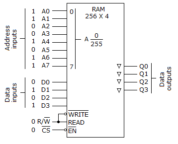
The RAM circuit given below is suspected of being bad. A check with a logic probe shows pulse activity on all of the address lines and data inputs. The / line and inputs are forced HIGH and the data output lines are checked with the logic probe. Q0, Q2, and Q3 show a dim indication on the logic probe; Q1 indicates a HIGH level on the logic probe. What, if anything, is wrong with the circuit?
Options- Correct Answer
- The Q1 line appears to be shorted to Vcc; replace the chip.
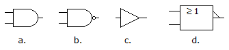
- 2. Which of the figures given below represents a NOR gate?
Options
Discuss
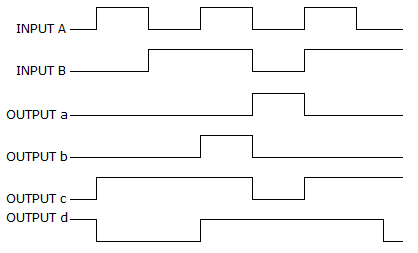
- 4. For a two-input XNOR gate, with the input waveforms as shown below, which output waveform is correct?
Options
Discuss
- 8. For the SOP expression
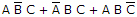 , how many 1s are in the truth table's output column?
Options
Discuss
More questions
Correct Answer: d
Correct Answer: d
Correct Answer: 3
Comments
There are no comments.