Discussion
Home ‣ Digital Electronics ‣ Memory and Storage See What Others Are Saying!
- Question
The condition occurring when two or more devices try to write data to a bus simultaneously is called ________.
Options- A. address decoding
- B. bus contention
- C. bus collisions
- D. address multiplexing
- Correct Answer
- bus contention
- 1. The output pulse width for a 555 monostable circuit with R1 = 3.3 kΩ and C1 = 0.02 µF is ________.
Options- A. 7.3 µs
- B. 73 µs
- C. 7.3 ms
- D. 73 ms Discuss
- 2. Which of the figures given below represents a NOR gate?

Options- A. a
- B. b
- C. c
- D. d Discuss
- 3. What is one advantage to using a parallel-encoded (flash) ADC?
Options- A. less expensive
- B. very fast conversion
- C. less complicated circuit Discuss
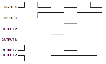
- 4. For a two-input XNOR gate, with the input waveforms as shown below, which output waveform is correct?

Options- A. a
- B. b
- C. c
- D. d Discuss
- 5. In a multiplexer, the data select control inputs are responsible for determining which data input is selected to be transmitted to the data output line.
Options- A. True
- B. False Discuss
- 6. The time required to complete a conversion cycle is called conversion time.
Options- A. True
- B. False Discuss
- 7. When more than one IC is used to provide all the addressable locations in a memory, a technique called ________ is used to identify which IC is being accessed.
Options- A. address decoding
- B. memory refresh
- C. data encoding
- D. memory paging Discuss
- 8. For the SOP expression
 , how many 1s are in the truth table's output column?
Options- A. 1
- B. 2
- C. 3
- D. 5 Discuss
- 9. A typical RAM will write (store data internally) whenever the Chip Select line is active and the Write Enable line is inactive.
Options- A. True
- B. False Discuss
- 10. The TTL HIGH level source current is higher than the LOW level sinking current.
Options- A. True
- B. False Discuss
More questions
Correct Answer: 73 µs
Correct Answer: d
Correct Answer: very fast conversion
Correct Answer: d
Correct Answer: True
Correct Answer: True
Correct Answer: address decoding
Correct Answer: 3
Correct Answer: False
Correct Answer: False
Comments
There are no comments.More in Digital Electronics:
Programming
Copyright ©CuriousTab. All rights reserved.
