logo

CuriousTab

CuriousTab

Discussion


Home Digital Electronics Integrated-Circuit Logic Families Comments

  • Question
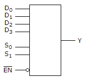
  • What type of circuit is represented in the given figure, and which statement best describes its operation?

    What type of circuit is represented in the given figure, and which statement best describes its oper


  • Options
  • A. It is a tristate inverter. When the ENABLE input is HIGH, the output is effectively an open circuit?it is neither LOW nor HIGH.
  • B. It is a programmable inverter. It can be programmed to function as either an active LOW or an active HIGH inverter.
  • C. It is an active LOW buffer, which can be turned on and off by the ENABLE input.
  • D. None of the above.

  • Correct Answer
  • It is a tristate inverter. When the ENABLE input is HIGH, the output is effectively an open circuit?it is neither LOW nor HIGH. 


  • Integrated-Circuit Logic Families problems


    Search Results


    • 1. What is unique about TTL devices such as the 74S00?

    • Options
    • A. The gate transistors are silicon (S), and the gates therefore have lower values of leakage current.
    • B. The S denotes the fact that a single gate is present in the IC rather than the usual package of 2?6 gates.
    • C. The S denotes a slow version of the device, which is a consequence of its higher power rating.
    • D. The devices use Schottky transistors and diodes to prevent them from going into saturation; this results in faster turn on and turn off times, which translates into higher frequency operation.
    • Discuss
    • 2. What must be done to interface TTL to CMOS?

    • Options
    • A. A dropping resistor must be used on the CMOS 12 V supply to reduce it to 5 V for the TTL.
    • B. As long as the CMOS supply voltage is 5 V, they can be interfaced; however, the fan-out of the TTL is limited to five CMOS gates.
    • C. A 5 V Zener diode must be placed across the inputs of the TTL gates in order to protect them from the higher output voltages of the CMOS gates.
    • D. A pull-up resistor must be used between the TTL output-CMOS input node and Vcc; the value of RP will depend on the number of CMOS gates connected to the node.
    • Discuss
    • 3. Refer the given figure. Which of the following describes the operation of the circuit?


    • Options
    • A. A LOW input turns Q1 and Q3 on; Q2 and Q4 are off.
    • B. A LOW input turns Q1 and Q4 off; Q2 and Q3 are on.
    • C. A HIGH input turns Q1, Q2, and Q3 off, and Q4 is on.
    • D. A HIGH input turns Q1, Q2, and Q4 on; Q3 is off.
    • Discuss
    • 4. Generally, the voltage measured at an unused TTL input would typically be measured between:

    • Options
    • A. 1.4 to 1.8 V.
    • B. 0 to 5 V.
    • C. 0 to 1.8 V.
    • D. 0.8 to 5 V.
    • Discuss
    • 5. What type of circuit is shown below, and how is the output ordinarily connected?


    • Options
    • A. It is an open-collector gate and is used to drive loads that cannot be connected directly to Vcc due to high noise levels.
    • B. It represents an active-LOW inverter and is used in negative logic systems.
    • C. It is an open-collector gate. An external load must be connected between the output terminal and an appropriate supply voltage.
    • D. Any of the above could be correct, depending on the specific application involved.
    • Discuss
    • 6. Which of the following summarizes the important features of ECL?

    • Options
    • A. Low noise margin, low output voltage swing, negative voltage operation, fast, and high power consumption
    • B. Good noise immunity, negative logic, high frequency capability, low power dissipation, and short propagation time
    • C. Slow propagation time, high frequency response, low power consumption, and high output voltage swings
    • D. Poor noise immunity, positive supply voltage operation, good low frequency operation, and low power
    • Discuss
    • 7. Logic circuits that are designated as buffers, drivers, or buffer/drivers are designed to have:

    • Options
    • A. a greater current/voltage capability than an ordinary logic circuit.
    • B. greater input current/voltage capability than an ordinary logic circuit.
    • C. a smaller output current/voltage capability than an ordinary logic.
    • D. greater input and output current/voltage capability than an ordinary logic circuit.
    • Discuss
    • 8. In an HDL stepper motor design, why is there more than one mode?

    • Options
    • A. To change the speed of the stepper motor
    • B. To change the direction of the stepper motor
    • C. To direct drive the stepper motor
    • D. All of the above
    • Discuss
    • 9. For the frequency counter, which is not a control signal from the control and timing block?

    • Options
    • A. Clear
    • B. Enable
    • C. Reset
    • D. Store
    • Discuss
    • 10. List three basic blocks in the digital clock project.

    • Options
    • A. MOD-60, MOD-12 counters
    • B. MOD-5, MOD-10, MOD-12 counters
    • C. MOD-60, MOD-10 counters
    • D. MOD-6, MOD-12, and MOD-10 counters
    • Discuss


    Comments

    There are no comments.

Enter a new Comment