logo

CuriousTab

CuriousTab

Discussion


Home Digital Electronics Integrated-Circuit Logic Families Comments

  • Question
  • Refer the given figure. Which of the following describes the operation of the circuit?
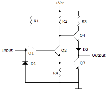
    Refer the given figure. Which of the following describes the operation of the circuit? A LOW input t


  • Options
  • A. A LOW input turns Q1 and Q3 on; Q2 and Q4 are off.
  • B. A LOW input turns Q1 and Q4 off; Q2 and Q3 are on.
  • C. A HIGH input turns Q1, Q2, and Q3 off, and Q4 is on.
  • D. A HIGH input turns Q1, Q2, and Q4 on; Q3 is off.

  • Correct Answer
  • A HIGH input turns Q1, Q2, and Q3 off, and Q4 is on. 


  • Integrated-Circuit Logic Families problems


    Search Results


    • 1. Generally, the voltage measured at an unused TTL input would typically be measured between:

    • Options
    • A. 1.4 to 1.8 V.
    • B. 0 to 5 V.
    • C. 0 to 1.8 V.
    • D. 0.8 to 5 V.
    • Discuss
    • 2. What type of circuit is shown below, and how is the output ordinarily connected?


    • Options
    • A. It is an open-collector gate and is used to drive loads that cannot be connected directly to Vcc due to high noise levels.
    • B. It represents an active-LOW inverter and is used in negative logic systems.
    • C. It is an open-collector gate. An external load must be connected between the output terminal and an appropriate supply voltage.
    • D. Any of the above could be correct, depending on the specific application involved.
    • Discuss
    • 3. What is the increase in switching speed between 74LS series TTL and 74HC/HCT (High-Speed CMOS)?

    • Options
    • A. 5
    • B. 10
    • C. 50
    • D. 100
    • Discuss
    • 4. A logic signal experiences a delay in going through a circuit. The two propagation delay times are defined as:

    • Options
    • A. tPLH and tPHL.
    • B. tDLH and tDHL.
    • C. tHPL and tlph.
    • D. tLDH and tHDL.
    • Discuss
    • 5. What type of circuit is shown below and which statement best describes its operation?


    • Options
    • A. It is a two-input CMOS AND gate with open drain.
    • B. It is a two-input CMOS buffer with tristate output.
    • C. It is a CMOS inverter with tristate output.
    • D. It is a hybrid TTL-CMOS inverter with FET totem-pole output.
    • Discuss
    • 6. What must be done to interface TTL to CMOS?

    • Options
    • A. A dropping resistor must be used on the CMOS 12 V supply to reduce it to 5 V for the TTL.
    • B. As long as the CMOS supply voltage is 5 V, they can be interfaced; however, the fan-out of the TTL is limited to five CMOS gates.
    • C. A 5 V Zener diode must be placed across the inputs of the TTL gates in order to protect them from the higher output voltages of the CMOS gates.
    • D. A pull-up resistor must be used between the TTL output-CMOS input node and Vcc; the value of RP will depend on the number of CMOS gates connected to the node.
    • Discuss
    • 7. What is unique about TTL devices such as the 74S00?

    • Options
    • A. The gate transistors are silicon (S), and the gates therefore have lower values of leakage current.
    • B. The S denotes the fact that a single gate is present in the IC rather than the usual package of 2?6 gates.
    • C. The S denotes a slow version of the device, which is a consequence of its higher power rating.
    • D. The devices use Schottky transistors and diodes to prevent them from going into saturation; this results in faster turn on and turn off times, which translates into higher frequency operation.
    • Discuss
    • 8. What type of circuit is represented in the given figure, and which statement best describes its operation?


    • Options
    • A. It is a tristate inverter. When the ENABLE input is HIGH, the output is effectively an open circuit?it is neither LOW nor HIGH.
    • B. It is a programmable inverter. It can be programmed to function as either an active LOW or an active HIGH inverter.
    • C. It is an active LOW buffer, which can be turned on and off by the ENABLE input.
    • D. None of the above.
    • Discuss
    • 9. Which of the following summarizes the important features of ECL?

    • Options
    • A. Low noise margin, low output voltage swing, negative voltage operation, fast, and high power consumption
    • B. Good noise immunity, negative logic, high frequency capability, low power dissipation, and short propagation time
    • C. Slow propagation time, high frequency response, low power consumption, and high output voltage swings
    • D. Poor noise immunity, positive supply voltage operation, good low frequency operation, and low power
    • Discuss
    • 10. Logic circuits that are designated as buffers, drivers, or buffer/drivers are designed to have:

    • Options
    • A. a greater current/voltage capability than an ordinary logic circuit.
    • B. greater input current/voltage capability than an ordinary logic circuit.
    • C. a smaller output current/voltage capability than an ordinary logic.
    • D. greater input and output current/voltage capability than an ordinary logic circuit.
    • Discuss


    Comments

    There are no comments.

Enter a new Comment