Discussion
Home ‣ Digital Electronics ‣ Integrated-Circuit Logic Families Comments
- Question
Which of the following will not normally be found on a data sheet?
Options- A. Minimum HIGH level output voltage
- B. Maximum LOW level output voltage
- C. Minimum LOW level output voltage
- D. Maximum HIGH level input current
- Correct Answer
- Minimum LOW level output voltage
- 1. A "floating" TTL input may be defined as:
Options- A. unused input that is tied to Vcc through a 1 k Ω resistor.
- B. unused input that is tied to used inputs.
- C. unused input that is tied to the ground.
- D. unused input that is not connected. Discuss
- 2. What must be done to interface CMOS to TTL?
Options- A. A dropping resistor must be used on the CMOS 12 V supply to reduce it to 5 V for the TTL.
- B. As long as the CMOS supply voltage is 5 V, they can be interfaced; however, the fan-out of the CMOS is limited to two TTL gates.
- C. A 5 V Zener diode must be placed across the inputs of the TTL gates in order to protect them from the higher output voltages of the CMOS gates.
- D. The two series cannot be interfaced without the use of special interface buffers designed for that purpose, such as the open-collector buffers. Discuss
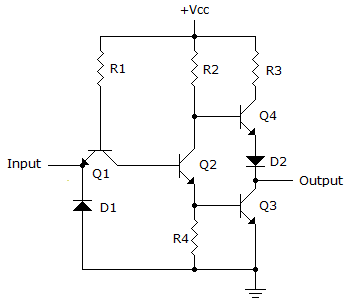
- 3. Refer to the given figure. What type of output arrangement is being used for the output?

Options- A. Complementary-symmetry
- B. Push-pull
- C. Quasi push-pull
- D. Totem-pole Discuss
- 4. The bipolar TTL logic family that was developed to increase switching speed by preventing transistor saturation is:
Options- A. emitter-coupled logic (ECL).
- B. current-mode logic (CML).
- C. transistor-transistor logic (TTL).
- D. emitter-coupled logic (ECL) and transistor-transistor logic (TTL). Discuss
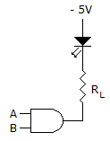
- 5. Refer to the figure given below. What type of device is shown and what input levels are required to turn the LED off?

Options- A. The device is an open-collector AND gate and requires both inputs to be HIGH in order to turn the LED off.
- B. The device is a Schottky AND gate and requires only one low input to turn the LED off.
- C. The device is an open-collector AND gate and requires only one low input to turn the LED off.
- D. The device is a Schottky open-collector AND gate and requires a low on both inputs to turn the LED off. Discuss
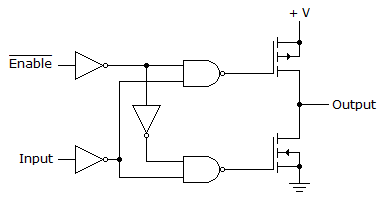
- 6. What type of circuit is shown below and which statement best describes its operation?

Options- A. It is a two-input CMOS AND gate with open drain.
- B. It is a two-input CMOS buffer with tristate output.
- C. It is a CMOS inverter with tristate output.
- D. It is a hybrid TTL-CMOS inverter with FET totem-pole output. Discuss
- 7. A logic signal experiences a delay in going through a circuit. The two propagation delay times are defined as:
Options- A. tPLH and tPHL.
- B. tDLH and tDHL.
- C. tHPL and tlph.
- D. tLDH and tHDL. Discuss
- 8. What is the increase in switching speed between 74LS series TTL and 74HC/HCT (High-Speed CMOS)?
Options- A. 5
- B. 10
- C. 50
- D. 100 Discuss
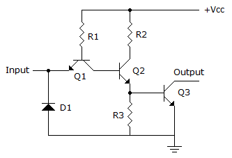
- 9. What type of circuit is shown below, and how is the output ordinarily connected?

Options- A. It is an open-collector gate and is used to drive loads that cannot be connected directly to Vcc due to high noise levels.
- B. It represents an active-LOW inverter and is used in negative logic systems.
- C. It is an open-collector gate. An external load must be connected between the output terminal and an appropriate supply voltage.
- D. Any of the above could be correct, depending on the specific application involved. Discuss
- 10. Generally, the voltage measured at an unused TTL input would typically be measured between:
Options- A. 1.4 to 1.8 V.
- B. 0 to 5 V.
- C. 0 to 1.8 V.
- D. 0.8 to 5 V. Discuss
Integrated-Circuit Logic Families problems
Search Results
Correct Answer: unused input that is not connected.
Correct Answer: As long as the CMOS supply voltage is 5 V, they can be interfaced; however, the fan-out of the CMOS is limited to two TTL gates.
Correct Answer: Totem-pole
Correct Answer: emitter-coupled logic (ECL) and transistor-transistor logic (TTL).
Correct Answer: The device is an open-collector AND gate and requires both inputs to be HIGH in order to turn the LED off.
Correct Answer: It is a CMOS inverter with tristate output.
Correct Answer: tPLH and tPHL.
Correct Answer: 10
Correct Answer: It is an open-collector gate. An external load must be connected between the output terminal and an appropriate supply voltage.
Correct Answer: 1.4 to 1.8 V.
Comments
There are no comments.More in Digital Electronics:
Programming
Copyright ©CuriousTab. All rights reserved.
