Discussion
Home ‣ Digital Electronics ‣ MSI Logic Circuits See What Others Are Saying!
- Question
Determine the correct output for the multiplexer and its associated timing diagram given below.
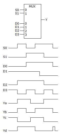
Options- A. Ya
- B. Yb
- C. Yc
- D. Yd
- Correct Answer
- Yd
- 1. The major blocks of the frequency counter are the counter, ________, decoder/display, and the timing and control unit.
Options- A. signal prescaler
- B. control inputs
- C. signal generator
- D. display register Discuss
- 2. Shift register counters use logic functions to reset the registers when the desired count is reached.
Options- A. True
- B. False Discuss
- 3. The software used to drive a microprocessor-based system is called FORTRAN.
Options- A. True
- B. False Discuss
- 4. The time delay called access time, tac, is a measure of the ROM's operating speed.
Options- A. True
- B. False Discuss
- 5. The 8051 has ________ 16-bit counter/timers.
Options- A. 1
- B. 2
- C. 3
- D. 4 Discuss
- 6. The CPU (Central Processing Unit) is composed of memory and outputs.
Options- A. True
- B. False Discuss
- 7. Using separate serial inputs for shifting left or shifting right is a major difference between the 74194 and other shift registers.
Options- A. True
- B. False Discuss
- 8. The time interval on the leading edge of a pulse between 10% and 90% of the amplitude is the rise time.
Options- A. True
- B. False Discuss
- 9. In the keypad HDL encoder, the ts bit array represents a tristate buffer.
Options- A. True
- B. False Discuss
- 10. ________ is a mature technology consisting of numerous subfamilies that have been developed over many years of use.
Options- A. TTL
- B. CMOS
- C. ECL
- D. None of the above Discuss
More questions
Correct Answer: display register
Correct Answer: False
Correct Answer: False
Correct Answer: False
Correct Answer: 2
Correct Answer: False
Correct Answer: True
Correct Answer: True
Correct Answer: True
Correct Answer: TTL
Comments
There are no comments.More in Digital Electronics:
Programming
Copyright ©CuriousTab. All rights reserved.