Discussion
Home ‣ Digital Electronics ‣ Integrated Circuit Technologies See What Others Are Saying!
- Question
Which logic family combines the advantages of CMOS and TTL?
Options- A. BiCMOS
- B. TTL/CMOS
- C. ECL
- D. TTL/MOS
- Correct Answer
- BiCMOS
- 1. A sample-and-hold circuit is used in D/A conversion.
Options- A. True
- B. False Discuss
- 2. The ________ is defined as the maximum number of standard logic inputs that an output can drive reliably.
Options- A. fan-drive
- B. fan-out
- C. fan-in
- D. open-collector Discuss
- 3. What is the difference between the 7476 and the 74LS76?
Options- A. the 7476 is master-slave, the 74LS76 is master-slave
- B. the 7476 is edge-triggered, the 74LS76 is edge-triggered
- C. the 7476 is edge-triggered, the 74LS76 is master-slave
- D. the 7476 is master-slave, the 74LS76 is edge-triggered Discuss
- 4. What is the major downfall of microprocessor/DSP systems?
Options- A. Speed?they are too fast
- B. Speed?they are too slow
- C. Too much flexibility
- D. Not enough flexibility Discuss
- 5. An 8-bit serial in/parallel out shift register is clocked at 4 MHz and is used to delay a serial digital signal by 1.25 µs. The output that has the proper delay is ________.
Options- A. QE
- B. QF
- C. QG
- D. QH Discuss
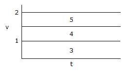
- 6. In a negative logic system, the area represented by #3 in the given figure would be the ________ level.

Options- A. HIGH
- B. LOW
- C. off
- D. uncertain Discuss
- 7. A 4-bit shift register that receives 4 bits of parallel data will shift to the ________ by ________ position(s) for each clock pulse.
Options- A. right, one
- B. right, two
- C. left, one
- D. left, three Discuss
- 8. How many different voltages can be output from a DAC with a 6-bit resolution?
Options- A. 6
- B. 16
- C. 32
- D. 64 Discuss
- 9. A 4-bit R/2R D/A converter has a reference of 5 V. What is the analog output for the input code 0101?
Options- A. 3.125 V
- B. 0.3125 V
- C. 0.78125 V
- D. ?3.125 V Discuss
- 10. A 0.01-µF capacitor is recommended by TTL manufacturers for ________ the power supply.
Options- A. decoupling
- B. filtering
- C. rectifying
- D. grounding Discuss
More questions
Correct Answer: False
Correct Answer: fan-out
Correct Answer: the 7476 is master-slave, the 74LS76 is edge-triggered
Correct Answer: Speed?they are too slow
Correct Answer: QE
Correct Answer: HIGH
Correct Answer: right, one
Correct Answer: 64
Correct Answer: ?3.125 V
Correct Answer: decoupling
Comments
There are no comments.More in Digital Electronics:
Programming
Copyright ©CuriousTab. All rights reserved.
