logo

CuriousTab

CuriousTab

Discussion


Home Digital Electronics Memory and Storage See What Others Are Saying!
  • Question
  • Refer the given figure. The outputs (Q0?Q3) of the memory are always LOW. The address lines (A0?A7) are checked with a logic probe and all are indicating pulse activity, except for A3, which shows a constant HIGH, and A7, which shows a constant LOW; the select lines, Refer the given figure. The outputs (Q0?Q3) of the memory are always LOW. The address lines (A0?A7) are checked and Refer the given figure. The outputs (Q0?Q3) of the memory are always LOW. The address lines (A0?A7) shows pulse activity, while Refer the given figure. The outputs (Q0?Q3) of the memory are always LOW. The address lines (A0?A7) indicates a constant HIGH. What is wrong, and how can the memory be tested to determine whether it is defective or if the external circuitry is defective?
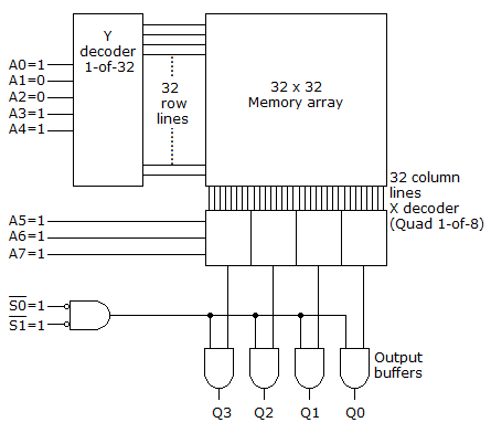
    Refer the given figure. The outputs (Q0?Q3) of the memory are always LOW. The address lines (A0?A7)


  • Options
  • A. One of the inputs to the active-LOW select AND gate may be stuck high for some reason; take both select lines LOW and check for pulse activity on the outputs, Q0?Q3. If the outputs now respond, the problem is most likely in the program or circuitry driving the select lines.
  • B. The problem appears to be in the two address lines that never change levels; the problem is probably in the program driving the memory address bus.
  • C. The output buffers are probably defective since they are all tied together; the common input line is most likely stuck LOW. Change the output buffer IC.
  • D. Since no data appears to be getting through to the output buffers, the problem may be in the X decoder; change the X decoder IC.

  • Correct Answer
  • One of the inputs to the active-LOW select AND gate may be stuck high for some reason; take both select lines LOW and check for pulse activity on the outputs, Q0?Q3. If the outputs now respond, the problem is most likely in the program or circuitry driving the select lines. 


  • More questions

    • 1. In a MAX7000S device, when an I/O pin is configured as an input, the associated macrocell can be used for ________.

    • Options
    • A. buried logic
    • B. another output
    • C. extra speed
    • D. in-system testing
    • Discuss
    • 2. A half-adder circuit would normally be used each time a carry input is required in an added circuit.

    • Options
    • A. True
    • B. False
    • Discuss
    • 3. A very important attribute of the conditional signal assignment statement is its sequential operation.

    • Options
    • A. True
    • B. False
    • Discuss
    • 4. In general, when using a scope to troubleshoot digital systems the instrument should be triggered by ________.

    • Options
    • A. the A channel or channel 1
    • B. the vertical input mode, when using more than one channel
    • C. the system clock
    • D. line sync, in order to observe troublesome power line glitches
    • Discuss
    • 5. Incandescent 7-segment displays are especially well suited for use in portable battery-operated devices.

    • Options
    • A. True
    • B. False
    • Discuss
    • 6. In BCD addition, the value ________ is added to any invalid code group.

    • Options
    • A. 010101
    • B. 0U812
    • C. 100110
    • D. 0110
    • Discuss
    • 7. In the 74121, which is nonretriggerable, any triggers that come in before the end of the timing cycle are ignored.

    • Options
    • A. True
    • B. False
    • Discuss
    • 8. SPLDs, CPLDs, and FPGAs are all which type of device?

    • Options
    • A. PAL
    • B. PLD
    • C. EPROM
    • D. SRAM
    • Discuss
    • 9. Gated S-R flip-flops are called asynchronous because the output responds immediately to input changes.

    • Options
    • A. True
    • B. False
    • Discuss
    • 10. A ROM that allows the user to program data into the chip by permanently opening fusible links is the EPROM.

    • Options
    • A. True
    • B. False
    • Discuss


    Comments

    There are no comments.

Enter a new Comment