Discussion
Home ‣ Digital Electronics ‣ Memory and Storage See What Others Are Saying!
- Question
What is the significance of the inverted triangles on the outputs of the device in the given figure?
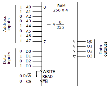
Options- A. They represent inverters and mean that the outputs are active-LOW.
- B. They represent buffers and mean that the outputs can drive 40 TTL loads, instead of the normal 10.
- C. It means that the outputs will be active only if a change has occurred at that memory location since the last read/write cycle.
- D. The outputs are tristated.
- Correct Answer
- The outputs are tristated.
- 1. In HDL, LITERALS is/are:
Options- A. digital systems.
- B. scalars.
- C. binary coded decimals.
- D. a numbering system. Discuss
- 2. Convert the following decimal number to hexadecimal.
74
Options- A. A416
- B. B416
- C. 4A16
- D. 4B16 Discuss
- 3. Most modern digital systems are based on semiconductor technology.
Options- A. True
- B. False Discuss
- 4. The BCD equivalent of 73 is 01001001.
Options- A. True
- B. False Discuss
- 5. The stepper motor HDL will ignore its counter inputs and pass control inputs directly to the output when set in mode ________.
Options- A. 1
- B. 2
- C. 3
- D. 4 Discuss
- 6. The CMOS uses bipolar transistors instead of MOSFET.
Options- A. True
- B. False Discuss
- 7. In TTL the noise margin is between 0.8 V and 0.4 V.
Options- A. True
- B. False Discuss
- 8. A very critical dimension in project management is the time your boss will give you to complete the HDL project.
Options- A. True
- B. False Discuss
- 9. The Boolean sum of the four product terms is called the sum-of-products.
Options- A. True
- B. False Discuss
- 10. How many flip-flops are required to construct a decade counter?
Options- A. 10
- B. 8
- C. 5
- D. 4 Discuss
More questions
Correct Answer: scalars.
Correct Answer: 4A16
Correct Answer: True
Correct Answer: False
Correct Answer: 1
Correct Answer: False
Correct Answer: True
Correct Answer: True
Correct Answer: True
Correct Answer: 4
Comments
There are no comments.More in Digital Electronics:
Programming
Copyright ©CuriousTab. All rights reserved.