CuriousTab
Search
CuriousTab
Home
Aptitude
Computer
C Programming
C# Programming
C++ Programming
Database
Java Programming
Networking
Engineering
Biochemical Engineering
Biochemistry
Biotechnology
Chemical Engineering
Civil Engineering
Computer Science
Digital Electronics
Electrical Engineering
Electronics
Electronics and Communication Engineering
Mechanical Engineering
Microbiology
Technical Drawing
GK
Current Affairs
General Knowledge
Reasoning
Data Interpretation
Logical Reasoning
Non Verbal Reasoning
Verbal Ability
Verbal Reasoning
Exams
AIEEE
Bank Exams
CAT
GATE
IIT JEE
TOEFL
Jobs
Analyst
Bank PO
Database Administrator
IT Trainer
Network Engineer
Project Manager
Software Architect
Discussion
Home
‣
Electronics
‣
Transistors and Applications
Comments
Question
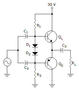
The maximum peak-to-peak output voltage in the given circuit is 15 V.
Options
A. True
B. False
Correct Answer
False
Transistors and Applications problems
Search Results
1. The voltage measured from the collector to the emitter is the sum of the voltage base-emitter plus the voltage collector-base.
Options
A. True
B. False
Show Answer
Scratch Pad
Discuss
Correct Answer: True
2. In an
n
-type JFET, current will flow when a positive voltage is applied to the drain and a negative voltage is applied to the source.
Options
A. True
B. False
Show Answer
Scratch Pad
Discuss
Correct Answer: True
3. An essential requirement of a feedback oscillator is a phase shift around the feedback loop of 360°.
Options
A. True
B. False
Show Answer
Scratch Pad
Discuss
Correct Answer: True
4. A practical CE amplifier has the input on the base and the output taken off the emitter.
Options
A. True
B. False
Show Answer
Scratch Pad
Discuss
Correct Answer: False
5. The
beta
of a BJT is the ratio of collector current to emitter current.
Options
A. True
B. False
Show Answer
Scratch Pad
Discuss
Correct Answer: False
6. If the drain, source, and channel of a MOSFET are all a
p
-type material, and it operates in both modes, this is an
n
-channel D-MOSFET.
Options
A. True
B. False
Show Answer
Scratch Pad
Discuss
Correct Answer: False
7. The power gain (
A
p
) of any transistor amplifier circuit equals the ___________.
Options
A. current gain squared
B. current gain times the voltage gain
C. voltage gain times the output resistance
D. current gain plus the voltage gain
Show Answer
Scratch Pad
Discuss
Correct Answer: current gain times the voltage gain
8. The collector current in a class A amplifier flows for ________ of the ac input signal.
Options
A. < 180°
B. 180°
C. < 360°
D. 360°
Show Answer
Scratch Pad
Discuss
Correct Answer: 360°
9. The ___ oscillator takes advantage of the
piezoelectric effect
.
Options
A. crystal
B. Hartley
C. Colpitts
D.
RC
Show Answer
Scratch Pad
Discuss
Correct Answer: crystal
10. The ac input resistance (
R
in
) of a voltage-divider biased common-emitter amplifier consists of ____________.
Options
A.
B.
C.
D.
Show Answer
Scratch Pad
Discuss
Correct Answer:
Comments
There are no comments.
Enter a new Comment
Save
More in Electronics:
Alternating Current and Voltage
Alternating Current vs Direct Current
Analog and Digital Converters
Analog to Digital
Arithmetic Operations and Circuits
Basic Op-Amp Circuits
Bipolar Junction Transistors (BJT)
Capacitors
Combinational Logic Circuits
Computer Hardware and Software
Diodes and Applications
Field Effect Transistors (FET)
Flip-Flops and Timers
Inductors
Logic Circuit Simplification
Logic Gates
Magnetism and Electromagnetism
Measurement, Conversion and Control
Number Systems and Codes
Ohm's Law
Operational Amplifiers
Parallel Circuits
Programmable Logic Devices (PLD)
Quantities and Units
RC Circuits
Resistance and Power
RL Circuits
RLC Circuits and Resonance
Semiconductor Memory
Semiconductor Principles
Sequential Logic Circuits
Series-Parallel Circuits
Series Circuits
Special-Purpose Op-Amp Circuits
Standard Logic Devices (SLD)
Testing and Troubleshooting
Thyristors and Tranducers
Time Response of Reactive Circuits
Transformers
Transistors and Applications
Voltage and Current