CuriousTab |
CuriousTab
Discussion
Home ‣ Electronics ‣ Standard Logic Devices (SLD) See What Others Are Saying!
- Question
Options- Correct Answer
- propagation delay
- 2.
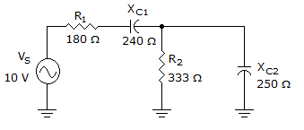
What is the phase angle in the given circuit?
Options
Discuss
- 6.

The phase angle in the circuit in the given circuit is approximately equal to ______.
Options
Discuss
- 8.
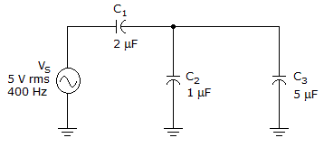
The total circuit reactance is ______ in the given circuit.
Options
Discuss
More questions
Correct Answer: 14.95°
Correct Answer: 37°
Correct Answer: 265 Ω
Comments
There are no comments.