logo

CuriousTab

CuriousTab

Discussion


Home Electronics Semiconductor Principles Comments

  • Question
  • In "p" type material, minority carriers would be:


  • Options
  • A. holes
  • B. dopants
  • C. slower
  • D. electrons

  • Correct Answer
  • electrons 

    Explanation
    The purpose of p-type doping is to create an abundance of holes. In the case of silicon, a trivalent atom (typically from Group 13 of the periodic table, such as boron or aluminium) is substituted into the crystal lattice. The result is that one electron is missing from one of the four covalent bonds normal for the silicon lattice. Thus the dopant atom can accept an electron from a neighboring atom's covalent bond to complete the fourth bond. This is why such dopants are called acceptors. The dopant atom accepts an electron, causing the loss of half of one bond from the neighboring atom and resulting in the formation of a "hole". Each hole is associated with a nearby negatively charged dopant ion, and the semiconductor remains electrically neutral as a whole. However, once each hole has wandered away into the lattice, one proton in the atom at the hole's location will be "exposed" and no longer cancelled by an electron. This atom will have 3 electrons and 1 hole surrounding a particular nucleus with 4 protons. For this reason a hole behaves as a positive charge. When a sufficiently large number of acceptor atoms are added, the holes greatly outnumber thermal excited electrons. Thus, holes are the majority carriers, while electrons become minority carriers in p-type materials.

  • Semiconductor Principles problems


    Search Results


    • 1. Which semiconductor material is made from coal ash?

    • Options
    • A. germanium
    • B. silicon
    • C. tin
    • D. carbon
    • Discuss
    • 2. Which of the following cannot actually move?

    • Options
    • A. majority carriers
    • B. ions
    • C. holes
    • D. free electrons
    • Discuss
    • 3. One problem with mechanically variable resistors is noticeable in audio circuits as:

    • Options
    • A. scratchy noise
    • B. lack of bass response
    • C. variable volume
    • D. too much treble response
    • Discuss
    • 4. With Ohm's law, no change in resistance means that current and voltage will be:

    • Options
    • A. directly proportional
    • B. unable to produce energy
    • C. the same
    • D. inversely proportional
    • Discuss
    • 5. A wire with a smaller cross-sectional area will produce:

    • Options
    • A. less heat
    • B. more conductance
    • C. less resistance
    • D. more heat
    • Discuss
    • 6. When an electron jumps from the valence shell to the conduction band, it leaves a gap. What is this gap called?

    • Options
    • A. energy gap
    • B. hole
    • C. electron-hole pair
    • D. recombination
    • Discuss
    • 7. Ionization within a P-N junction causes a layer on each side of the barrier called the:

    • Options
    • A. junction
    • B. depletion region
    • C. barrier voltage
    • D. forward voltage
    • Discuss
    • 8. Silicon atoms combine into an orderly pattern called a:

    • Options
    • A. covalent bond
    • B. crystal
    • C. semiconductor
    • D. valence orbit
    • Discuss
    • 9. Which material may also be considered a semiconductor element?

    • Options
    • A. carbon
    • B. ceramic
    • C. mica
    • D. argon
    • Discuss
    • 10. What is the voltage across R1 if the P-N junction is made of silicon?
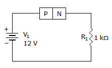

    • Options
    • A. 12 V
    • B. 11.7 V
    • C. 11.3 V
    • D. 0 V
    • Discuss


    Comments

    There are no comments.

Enter a new Comment