CuriousTab |
CuriousTab
Discussion
Home ‣ Electronics and Communication Engineering ‣ Electronic Devices and Circuits Comments
- Question
Options- Correct Answer
- False
ExplanationWith increase in temperature width of depletion layer decreases.
Electronic Devices and Circuits problems
Search Results
Options
Discuss
Correct Answer: 42.53, 0.85 ?A
Explanation:
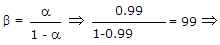
SICO = (1 + ?).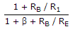
⟹ 51.
 = 42.53
 ?IC = (SICO).?ICO
= 42.53 x 19.9 nA
= 0.85 ?A.
Options
Discuss
Correct Answer: 100
Explanation:
 Current gain = 1 + ? = 100.
Options
Discuss
Correct Answer: 1/11 k?
Explanation:
Input Resistance with feedback for current shunt, .
.
Options
Discuss
Correct Answer: class B O/P stage
Explanation:
It is a characteristics of class B output stage as the amplifier is biased in cut-off region.In class B amplifier, two transistor are operated in such a way that one is amplify the half cycle and second is amplify -ve half cycle.
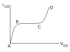
- 10. The v-i characteristics of a FET is shown in figure. In which region is the device biased for small signal amplification
Options
Discuss
Correct Answer: BC
Explanation:
Small signal amplifier operation is in constant current region of characteristics.
Comments
There are no comments.