logo

CuriousTab

CuriousTab

Discussion


Home Electronics and Communication Engineering Electronic Devices and Circuits Comments

  • Question
  • A transistor has a current gain of 0.99 in the CB mode. Its current gain in the CC mode is


  • Options
  • A. 100
  • B. 99
  • C. 1.01
  • D. 0.99

  • Correct Answer
  • 100 

    Explanation
    A transistor has a current gain of 0.99 in the CB mode. Its current gain in the CC mode is 100 99 1. 
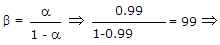
Current gain = 1 + ? = 100.

    Electronic Devices and Circuits problems


    Search Results


    • 1. A transistor has two p-n junctions. The batteries should be connected such that

    • Options
    • A. both junctions are forward biased
    • B. both junctions are reverse biased
    • C. one junction is forward biased and the other is reverse biased
    • D. none of the above
    • Discuss
    • 2. Assertion (A): The conductivity of p type semiconductor is higher than that of intrinsic semiconductor.

      Reason (R): The addition of donor impurity creates additional energy levels below conduction band.


    • Options
    • A. Both A and R are true and R is correct explanation of A
    • B. Both A and R are true but R is not a correct explanation of A
    • C. A is true but R is false
    • D. A is false but R is true
    • Discuss
    • 3. In a bipolar transistor which current is largest

    • Options
    • A. collector current
    • B. base current
    • C. emitter current
    • D. base current or emitter current
    • Discuss
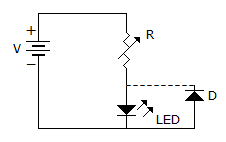
    • 4. In the circuit of figure the function of resistor R and diode D are
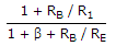
    • Options
    • A. to limit the current and to protect LED against over voltage
    • B. to limit the voltage and to protect LED against over current
    • C. to limit the current and protect LED against reverse breakdown voltage.
    • D. none of the above.
    • Discuss
    • 5. At room temperature the current in an intrinsic semiconductor is due to

    • Options
    • A. holes
    • B. electrons
    • C. ions
    • D. holes and electrons
    • Discuss
    • 6. A p-n junction diode has

    • Options
    • A. low forward and high reverse resistance
    • B. a non-linear v-i characteristics
    • C. zero forward current till the forward voltage reaches cut in value
    • D. all of the above
    • Discuss
    • 7. Assertion (A): The reverse saturation current in a semiconductor diode is 4nA at 20°C and 32 nA at 50°C.

      Reason (R): The reverse saturation current in a semiconductor diode doubles for every 10°C rise in temperature.


    • Options
    • A. Both A and R are true and R is correct explanation of A
    • B. Both A and R are true but R is not a correct explanation of A
    • C. A is true but R is false
    • D. A is false but R is true
    • Discuss
    • 8. Calculate the stability factor and change in IC from 25°C to 100°C for, ? = 50, RB/ RE = 250, ?IC0 = 19.9 nA for emitter bias configuration.

    • Options
    • A. 42.53, 0.85 ?A
    • B. 40.91, 0.58 ?A
    • C. 40.91, 0.58 ?A
    • D. 41.10, 0.39 ?A
    • Discuss
    • 9. An increase in temperature increases the width of depletion layer.

    • Options
    • A. True
    • B. False
    • Discuss
    • 10. An amplifier without feedback has a voltage gain of 50, input resistance of 1 k? and output resistance of 2.5 k?. The input resistance of the current shunt -ve feedback amplifier using the above amplifier with a feedback factor of 0.2 is

    • Options
    • A. 1/11 k?
    • B. 1/5 k?
    • C. 5 kW
    • D. 11 kW
    • Discuss


    Comments

    There are no comments.

Enter a new Comment