CuriousTab
CuriousTab
Home
Aptitude
Computer
C Programming
C# Programming
C++ Programming
Database
Java Programming
Networking
Engineering
Biochemical Engineering
Biochemistry
Biotechnology
Chemical Engineering
Civil Engineering
Computer Science
Digital Electronics
Electrical Engineering
Electronics
Electronics and Communication Engineering
Mechanical Engineering
Microbiology
Technical Drawing
GK
Current Affairs
General Knowledge
Reasoning
Data Interpretation
Logical Reasoning
Non Verbal Reasoning
Verbal Ability
Verbal Reasoning
Exams
AIEEE
Bank Exams
CAT
GATE
IIT JEE
TOEFL
Jobs
Analyst
Bank Clerk
Bank PO
Database Administrator
IT Trainer
Network Engineer
Project Manager
Software Architect
Discussion
Home
‣
Electronics and Communication Engineering
‣
Power Electronics
See What Others Are Saying!
Question
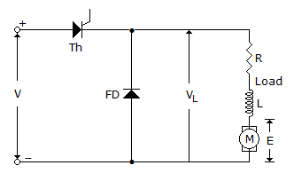
Figure shows a chopper feeding RLE load, The free wheeling diode conducts when
Options
A. thyristor is on
B. thyristor is off
C. both when thyristor is on and thyristor is off
D. partly when thyristor is off and partly when thyristor is on
Correct Answer
thyristor is off
Explanation
FD is forward biased only when thyristor is off.
More questions
1. The output frequency of a cycloconverter can be changed by changing the firing angle.
Options
A. True
B. False
Show Answer
Scratch Pad
Discuss
Correct Answer: False
2. Most of the memory chips in static RAM
Options
A. do not require any supply
B. need 2 V supply
C. need 5 V supply
D. need 12 V supply
Show Answer
Scratch Pad
Discuss
Correct Answer: need 5 V supply
Explanation:
Digital chips need 5 V supply.
3. In crystalline solids, atoms are stacked in a regular manner.
Options
A. True
B. False
Show Answer
Scratch Pad
Discuss
Correct Answer: True
4. The classes of solid dielectrics are
Options
A. A, B, C, D, E, F, H
B. A E B F H C D
C. Y A E B F H C
D. A E B F H C
Show Answer
Scratch Pad
Discuss
Correct Answer: Y A E B F H C
5. The unit for mmf is
Options
A. A
B. Wb
C. T
D. V
Show Answer
Scratch Pad
Discuss
Correct Answer: A
6. In a single phase full wave regulator, the firing angles in the positive and negative half cycles are generally
Options
A. equal
B. different
C. equal or different
D. different but sometimes equal
Show Answer
Scratch Pad
Discuss
Correct Answer: equal
Explanation:
Firing angles are kept equal to get symmetrical output voltage.
7. The real part of complex dielectric constant and tan? for a dielectric are 2.1 and 5 x 10
-4
at 100 Hz respectively. The imaginary part of dielectric constant at 100 Hz is
Options
A. 1.05 x 10
-3
B. 2.1 x 10
-3
C. 5 x 10
-3
D. 1.05 x 10
-2
Show Answer
Scratch Pad
Discuss
Correct Answer: 1.05 x 10
-3
Explanation:
8. The units for ?
r
are
Options
A. Farads
B. Farads/m
C.
D. no units
Show Answer
Scratch Pad
Discuss
Correct Answer: no units
Explanation:
?
r
is only a numeric. Hence no units.
9. Tesla is a unit of
Options
A. flux
B. field strength
C. flux density
D. MMF
Show Answer
Scratch Pad
Discuss
Correct Answer: flux density
10. In a receiver, which of the following device has IF input but RF output?
Options
A. Demodulator
B. Loudspeaker
C. Audio amplifier
D. Frequency changer
Show Answer
Scratch Pad
Discuss
Correct Answer: Demodulator
Comments
There are no comments.
Enter a new Comment
Save
More in Electronics and Communication Engineering:
Analog Electronics
Automatic Control Systems
Communication Systems
Digital Electronics
Electromagnetic Field Theory
Electronic Devices and Circuits
Exam Questions Papers
Matching Questions
Materials and Components
Measurements and Instrumentation
Microprocessors
Microwave Communication
Networks Analysis and Synthesis
Power Electronics
Radio Receivers
Satellite Communication
Signals and Systems