Discussion
Home ‣ Electronics and Communication Engineering ‣ Electronic Devices and Circuits See What Others Are Saying!
- Question
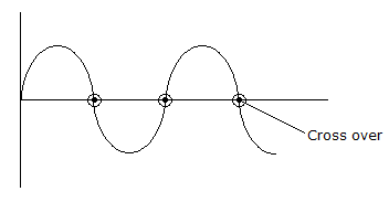
Crossover distortion behaviour is characteristic of
Options- A. class A O/P stage
- B. class B O/P stage
- C. class AB output stage
- D. common pulse O/P state
- Correct Answer
- class B O/P stage
ExplanationIt is a characteristics of class B output stage as the amplifier is biased in cut-off region.In class B amplifier, two transistor are operated in such a way that one is amplify the half cycle and second is amplify -ve half cycle.

More questions
- 1. As compared to dimensions of most feeds, the skin depth at microwave frequencies is
Options- A. of the same magnitude
- B. much larger
- C. much smaller
- D. either (b) or (c) Discuss
Correct Answer: of the same magnitude
- 2. For a 1 cm x 2 cm air filled rectangular waveguide the maximum frequency should be less than about
Options- A. 1000 MHz
- B. 5000 MHz
- C. 14000 MHz
- D. 140000 MHz Discuss
Correct Answer: 14000 MHz
- 3. In a radio receiver
Options- A. all stages contribute equally to noise
- B. RF stage has no effect on S/N ratio
- C. mixer stage contributes most of the noise generated Discuss
Correct Answer: mixer stage contributes most of the noise generated
- 4. As compared to an ordinary semiconductor diode, a Schottky diode
Options- A. has higher reverse saturation current
- B. has higher reverse saturation current and higher cut in voltage
- C. has higher reverse saturation current and lower cut in voltage
- D. has lower reverse saturation current and lower cut in voltage Discuss
Correct Answer: has higher reverse saturation current and lower cut in voltage
Explanation:
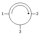
This is due to high electron concentration in metals.- 5. A 3 port circulator is in the given figure. Its scattering matrix is

Options- A.

- B.

- C.

- D.
 Discuss
Correct Answer:
- 6. The total field developed by an antenna array at a distant point is
Options- A. phasor sum of fields produced by individual antennas of the array
- B. algebraic sum of fields produced by individual antennas of the array
- C. either (a) or (b) depending on type of array
- D. neither (a) nor (b) Discuss
Correct Answer: phasor sum of fields produced by individual antennas of the array
Explanation:
Since field is a phasor quantity we have to take phasor sum.- 7. A standard cell of 1.0185 V is used with a slide wire potentiometer. The balance was obtained at 60 cm. When an unknown emf was connected, the balance was obtained at 82 cm. The magnitude of unknown emf is
Options- A. 1.39 V
- B. 0.75 V
- C. 13.9 V
- D. 7.45 V Discuss
Correct Answer: 1.39 V
Explanation:
 .
.
- 8. The number of valence electrons in donor impurity are
Options- A. 5
- B. 4
- C. 3
- D. 1 Discuss
Correct Answer: 5
Explanation:
Donor impurity has 5 valence electrons (while silicon has 4 valence electrons).Hence donor impurity can donate electrons.
- 9. Assertion (A): A DIAC has four layers but only two terminals.
Reason (R): A DIAC can conduct in both directions.
Options- A. Both A and R are correct and R is correct explanation of A
- B. Both A and R correct but R is not correct explanation of A
- C. A is correct but R is wrong
- D. A is wrong but R is correct Discuss
Correct Answer: Both A and R correct but R is not correct explanation of A
- 10. A NAND gate has 3 inputs and one output. The number of thyristors required for this gate are
Options- A. 1
- B. 2
- C. 3
- D. 3 or 4 Discuss
Correct Answer: 3
Comments
There are no comments.
More in Electronics and Communication Engineering:
Programming
Copyright ©CuriousTab. All rights reserved.
