CuriousTab |
CuriousTab
Discussion
Home ‣ Electronics and Communication Engineering ‣ Analog Electronics Comments
- Question
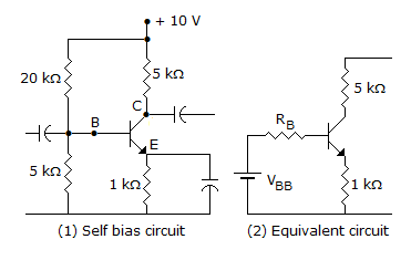
Figure shows the self bias circuit for CE amplifier and its equivalent circuit. VBB and RB respectively are
Options- Correct Answer
- 2 V and 4 k ohm
Explanation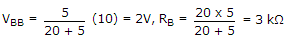 .
.
Analog Electronics problems
Search Results
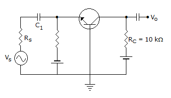
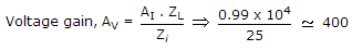
- 5. The 'h' parameters of the circuit shown in the figure are hib = 25 ?, hfb = 0.999 and hob = 10-6? The Voltage gain is
Options
Discuss
Correct Answer: 4
Explanation:
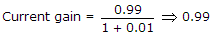
Zi = 25 + 10-6 x 0.99 x 104 ⟹ 25
 .
.
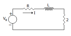
- 6. In a circuit of figure, Vs = 10 cos(?t) power drawn by the 2? resistor is 4 watts. The power factor is
Options
Discuss
Correct Answer: 0.6
Explanation:
Vs = 10 cos ?t,Let I be the current, then P = I2 R
I is the rms current.
⟹ Prms =
 I2 R ⟹ 4 ⟹ I2 = 4 ⟹ I = 2A.
Total power drawn =
Vm Im cos ?⟹
10 x 2 cos ? = 10 cos ?Total power cannot be determine until value of R = 12 ? is given.
- 5. The 'h' parameters of the circuit shown in the figure are hib = 25 ?, hfb = 0.999 and hob = 10-6? The Voltage gain is

 .
.