logo

CuriousTab

CuriousTab

Discussion


Home Digital Electronics Memory and Storage Comments

  • Question
  • Describe the timing diagram of a write operation.


  • Options
  • A. First the data is set on the data bus and the address is set, then the write pulse stores the data.
  • B. First the address is set, then the data is set on the data bus, and finally the read pulse stores the data.
  • C. First the write pulse stores the data, then the address is set, and finally the data is set on the data bus.
  • D. First the data is set on the data bus, then the write pulse stores the data, and finally the address is set.

  • Correct Answer
  • First the data is set on the data bus and the address is set, then the write pulse stores the data. 


  • Memory and Storage problems


    Search Results


    • 1. Microprocessors and memory ICs are generally designed to drive only a single TTL load. Therefore, if several inputs are being driven from the same bus, any memory IC must be ________.

    • Options
    • A. buffered
    • B. decoded
    • C. addressed
    • D. stored
    • Discuss
    • 2. ROMs retain data when the ________.

    • Options
    • A. power is off
    • B. power is on
    • C. system is down
    • D. all of the above
    • Discuss
    • 3. The refresh period for capacitors used in DRAMs is ________.

    • Options
    • A. 2 ms
    • B. 2 µs
    • C. 64 ms
    • D. 64 µs
    • Discuss
    • 4. When a RAM module passes the checkerboard test it is:

    • Options
    • A. able to read and write only 1s.
    • B. faulty.
    • C. probably good.
    • D. able to read and write only 0s.
    • Discuss
    • 5. Which type of ROM can be erased by UV light?

    • Options
    • A. ROM
    • B. mask ROM
    • C. EPROM
    • D. EEPROM
    • Discuss
    • 6. Which of the following RAM timing parameters determine its operating speed?

    • Options
    • A. tACC
    • B. tAA and tACS
    • C. tCO and tOD
    • D. tRC and tWC
    • Discuss
    • 7. The main advantage of semiconductor RAM is its ability to:

    • Options
    • A. retain stored data when power is interrupted or turned off
    • B. be written to and read from rapidly
    • C. be randomly accessed
    • D. be sequentially accessed
    • Discuss
    • 8. In general, the ________ have the smallest bit size and the ________ have the largest.

    • Options
    • A. EEPROMs, Flash
    • B. SRAM, mask ROM
    • C. mask ROM, SRAM
    • D. DRAM, PROM
    • Discuss
    • 9. The ideal memory ________.

    • Options
    • A. has high storage capacity
    • B. is nonvolatile
    • C. has in-system read and write capacity
    • D. has all of the above characteristics
    • Discuss
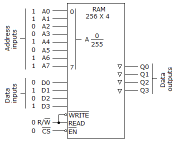
    • 10. What is the significance of the inverted triangles on the outputs of the device in the given figure?


    • Options
    • A. They represent inverters and mean that the outputs are active-LOW.
    • B. They represent buffers and mean that the outputs can drive 40 TTL loads, instead of the normal 10.
    • C. It means that the outputs will be active only if a change has occurred at that memory location since the last read/write cycle.
    • D. The outputs are tristated.
    • Discuss


    Comments

    There are no comments.

Enter a new Comment